
This weeks assignment was to make an In-Circuit Programmer by milling and stuffing and further testing its operations.
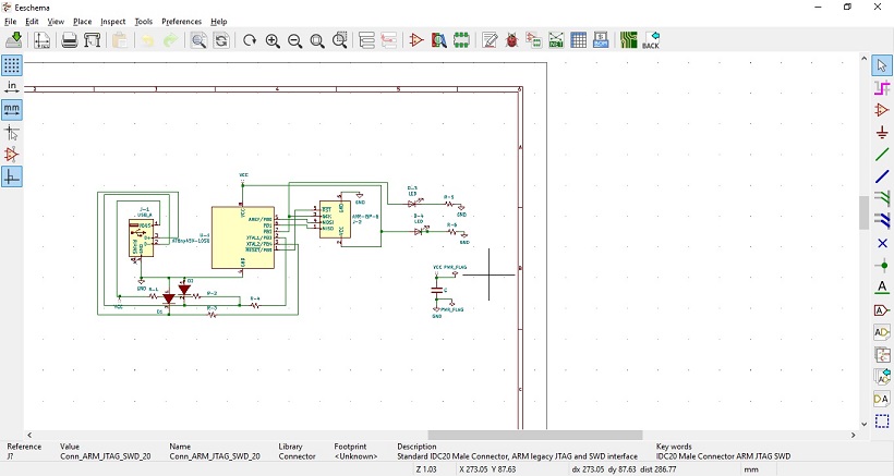
To design an In-circuit programmer, I have used KiCad software. I had used this software during my Pre FAB Academy Training and hence was comfortable with it. To start with, it was required to make schematic diagram of my In-circuit Programmer. The components used for making the schematic diagram are as under:-
1. Attiny-45
2. AVR ISP-6
3. USB
4. Diodes
5.Resistors
6. LEDs
As per the class on 19.02.2020, it was asked to make the In-circuit Programmer using UPDI or JTAG (ARM) instead of ISP but the library of my Kicad software is showing neither of two. The library is not updating as well. Hence, I need to troubleshoot my kicad software after which I can design my circuit board as required. But in the mean time for completing the individual assignment I have used ISP-6. The schematic diagram of my circuit is shown in the image below:-
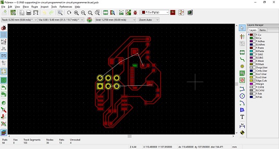
After the completion of my schematic diagram, it was require to perform following steps with the prepared schematic:-
Step-1:- Annotate PCB foot prints.
Step-2:-Perform Electrical rule check. This step will show the errors as per electrical check rules which are to be removed as per the instructions for proceeding further.
Step-3- Assign PCB Foot Prints to the schematic.
Step-4- Run PCB New to layout printed circuit board. This step can only be performed when the steps from 1 to 3 are executed and all errors are removed. In this step, our schematic would be converted into a PCB borad with all the components selected in the schematic.
Step-5:- In this step the connections shown in white are to be connected as per the directions of the software which would make the traces and cut file of our PCB. Further this step also shown the orientation and connection of our components in the pcb.
The pcb design of my In-circuit Programmer is shown in the image below:-
Further the image has to be saved in .png format which would be used by mods to prepare a trace and cut file. The trace and cut file of the pcb is shown below:-
Trace File:-
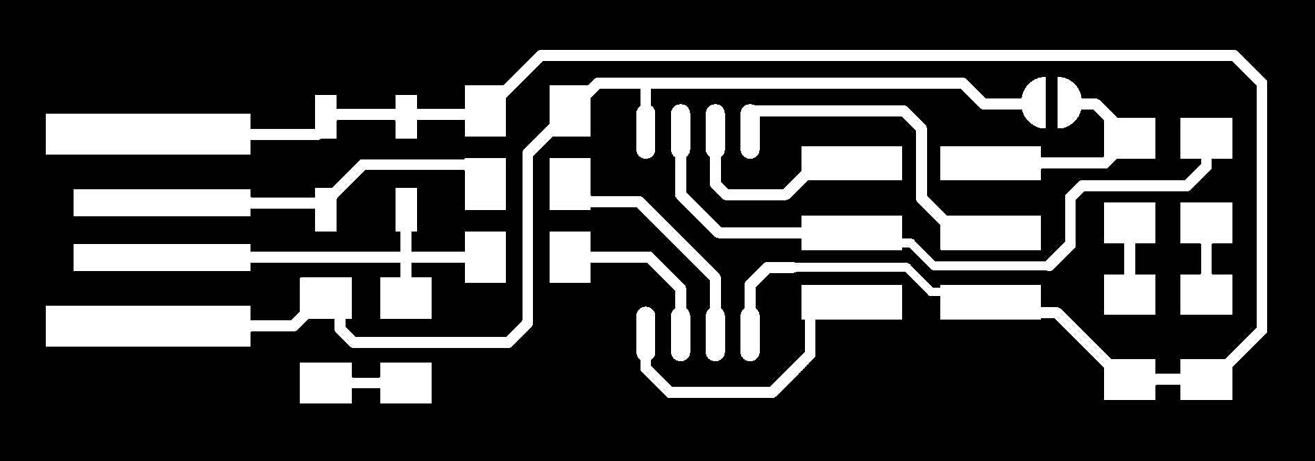
Cut File:-

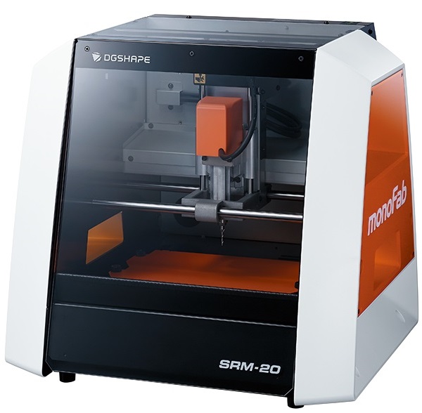
Now, these images can be traced and milled in SRM-20, the desktop milling machine installed at FAB LAB, STPI Bhubaneswar.
Milling bits are used to create traces and cuts in the PCB in following ways:-
1) For making traces milling bit of 1/64 is used.
2) For cutting the PCB bit of 1/32 is used.
For the use of SRM-20 desktop milling machine, V-pannel Controller software of SRM-20 is used. The controller is easy to use and operate the desktop milling machine. In the v-panel, the x, y and z axis is to be set so that milling and cutting is defined by the user. as per the v-panel, there are 2 origins. One is of the machine and other is user defined. The setting of origin in x, y and z axis is under in the user defined mode and subsequently the x, y and z axis of machine is also noted for safety purpose that in case the user defined origin is mismatched the values of x,y and z coordinates of machines may be used to bring the machine to the desired origin.
With respect to the milling and component soldering in my PCB, a technical issue has been caused due to which the SRM-20 is not working. The Z-plane of the machine is locked and hence the machine is not operating. The issue is under resolution and I would complete the assignment as soon as the technical issue with the machine is fixed.